Phosphor Tubes vs. CMOS Sensors: A Technical Deep Dive into Night Vision Technology
Analog night vision has relied on phosphor-based image intensifier tubes for 60 years. Modern CMOS sensors take a fundamentally different path to the same goal. Here's exactly how each technology works—and where the gap now stands.

Night vision devices all share the same challenge: extracting useful images from photon-starved environments. But the two dominant technologies—analog image intensifier tubes (IIT) and digital CMOS sensors—solve that problem through completely different physical mechanisms. Understanding those mechanisms explains not just which is "better," but why, and for whom.
How an Image Intensifier Tube (Phosphor) Works
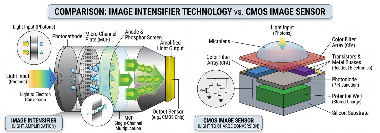
A Gen 2 or Gen 3 image intensifier is essentially a vacuum tube with three active stages:
Stage 1: The Photocathode
Incoming photons strike a photocathode—a thin semiconductor film (typically gallium arsenide, GaAs, in Gen 3) deposited on the inside of the input window. Through the photoelectric effect, each absorbed photon can eject a single electron. The efficiency of this conversion is called quantum efficiency (QE). Gen 3 GaAs photocathodes achieve QE values of 30–40% in the 600–900nm range, peaking in the near-infrared.
The photocathode is the core determinant of Gen 3 performance. It is also the component that is permanently damaged by bright light exposure: a photon flood causes excessive electron emission, which heats and chemically degrades the photocathode surface—damage that cannot be repaired.
Stage 2: The Microchannel Plate (MCP)
Electrons emitted by the photocathode are accelerated by a high-voltage field (~200V) toward the microchannel plate—a thin glass disk perforated with millions of microscopic channels (typically 6–10μm diameter). As each electron travels through a channel, it strikes the channel walls, releasing secondary electrons in a cascade. A single input electron produces 10,000 to 50,000 output electrons. This is the gain stage.
MCP quality directly determines signal-to-noise ratio. A high-quality MCP ("filmless" or "thin-filmed" variants) minimizes background thermal electron emission (dark current) to improve contrast in near-total darkness. This is the specification variance that makes some PVS-14 tubes worth $3,500 and others worth $8,000.
Stage 3: The Phosphor Screen
Amplified electrons strike a phosphor screen (P43 yellow-green phosphor for Gen 2/3, P45 white phosphor for white phos variants), producing visible light photons. The eye then receives this output through the eyepiece optics.
The characteristic green image is not an arbitrary aesthetic choice—P43 phosphor emission peaks near 543nm, which happens to match the peak spectral sensitivity of human scotopic (low-light) vision. White phosphor P45 trades some brightness for improved resolution and contrast perception, which is why operators willing to pay a premium prefer it.
IIT Limitations
- Dynamic range: roughly 10,000:1 (limited by MCP saturation)
- Spectral response: limited to approximately 450–900nm; blind beyond 900nm
- Fragility: irreversible photocathode damage from bright light
- Latency: near-zero (electron transit is essentially instantaneous)
- No digital output: cannot record, stream, or digitally process the image
- Cost: a quality MCP + GaAs photocathode assembly costs $2,000–$6,000 to manufacture
How a CMOS Sensor Works
A CMOS (Complementary Metal-Oxide-Semiconductor) image sensor replaces the entire vacuum tube chain with solid-state silicon electronics. Each pixel is an independent photodetector.
The Photodiode and Pixel Well
Each pixel contains a reverse-biased photodiode. When a photon is absorbed by the silicon, it generates an electron-hole pair through the photoelectric effect (the same principle as a photocathode, but in silicon). The electron is collected and stored in the pixel's potential well—a region with a defined charge capacity called the full-well capacity (FWC).
The number of photons that can be accumulated before the well overflows (saturates) determines the sensor's exposure ceiling. The noise floor—dominated by read noise and dark current—determines the minimum detectable signal. The ratio of FWC to noise floor is the dynamic range.
Pixel Size Is Everything
Larger pixels have two key advantages in low-light imaging:
- More photon collection area: a pixel's signal scales with its area. An 18μm pixel collects approximately 9× more photons per unit time than a 6μm pixel under the same illumination.
- Higher full-well capacity: larger physical pixels can accumulate more charge before saturating, increasing dynamic range ceiling.
This is why the ASTRA-X10 uses an 18μm pixel pitch—one of the largest pixel pitches in any production night vision sensor. Combined with a 1-inch optical format and an F1.05 objective lens (one of the fastest available), the system collects an exceptional photon flux per pixel compared to smaller-format sensors with tighter pixel pitches.
Back-Side Illumination (BSI)
In a conventional front-side illuminated (FSI) CMOS sensor, the wiring layers (metal interconnects, transistors) sit above the silicon photodiode—physically blocking some of the incoming light. Back-side illumination (BSI) flips the pixel stack: the photodiode faces the incoming light directly, with circuitry on the back. This improves quantum efficiency by 30–50% in the near-infrared region critical to night vision, and reduces optical cross-talk between adjacent pixels.
The Astra sensor architecture uses BSI construction for exactly this reason: maximizing photon capture efficiency without increasing pixel size.
Spectral Response: A Key CMOS Advantage
Silicon photodiodes respond to light from approximately 400nm to 1100nm—covering the full visible spectrum and extending deep into the near-infrared (NIR). This is significantly broader than a Gen 3 GaAs photocathode, which rolls off above 900nm.
The practical consequence: a CMOS sensor can image IR laser designators, IR illuminators, and NIR-reflective scenes that are invisible to analog IIT systems. The ASTRA-X10's 400–1100nm spectral response captures approximately 40% more of the near-infrared spectrum than a typical Gen 3 tube—particularly relevant for users who work with 940nm-band IR illuminators or laser systems.
The ISP and Digital Processing Chain
Raw sensor output is analog voltage. An on-chip or dedicated image signal processor (ISP) handles analog-to-digital conversion, noise reduction, gamma correction, and frame output. The ISP is where digital night vision has historically lagged and has recently made the most progress.
Processing latency—the time from photon capture to display output—is a function of pipeline depth and clock speed. At 100 frames per second, each frame has a maximum pipeline window of 10ms. The ASTRA-X10 achieves sub-10ms end-to-end latency at 100Hz, which is imperceptible during normal head movement (vestibulo-ocular reflex compensation begins to fail above approximately 40–50ms).
Technical Comparison: IIT vs. CMOS
| Parameter | Gen 3 IIT (Analog) | ASTRA-X10 CMOS (Digital) |
|---|---|---|
| Spectral range | 450–900nm | 400–1100nm |
| Minimum illumination | ~0.001 Lux (auto-gated) | 0.00005 Lux |
| Bright-light safe | No — permanent damage risk | Yes — solid state |
| Latency | Near-zero (electron transit) | <10ms at 100fps |
| Video recording | No | Yes — onboard storage |
| IR laser visibility | Limited above 900nm | Full coverage to 1100nm |
| Dynamic range | ~10,000:1 | HDR via LOFIC (see below) |
| Repairability | Specialized vacuum tube service | Standard electronics repair |
| Export control | ITAR restricted | EAR99 / unrestricted |
| Entry price | $3,000–$10,000+ | $999–$1,199 |
Where the Gap Remains
Analog IIT maintains advantages in two specific areas:
1. Absolute sensitivity in zero-illumination environments. A high-quality Gen 3 tube with auto-gating can operate in near-total darkness where even passive ambient photons are sparse. CMOS sensors require some photon flux to build a signal above thermal noise. In practice, this matters only at the extreme low end—overcast moonless nights with no IR illumination. At 0.00005 Lux, the ASTRA-X10 operates well below the human eye's threshold and below most practical night environments.
2. Latency under extreme conditions. While <10ms is imperceptible in normal use, an IIT produces effectively zero latency at any frame rate because it is an analog optical process. For helicopter pilots or certain military applications where even microsecond delays in visual feedback matter, analog IIT remains the reference standard.
The Bottom Line
For the vast majority of users—hunters, outdoor professionals, security operators, first responders, and enthusiasts—modern CMOS technology matches or surpasses analog IIT performance while eliminating its most significant practical drawbacks. The 1-inch large-pixel BSI CMOS sensor in the ASTRA-X10 represents the current state of the art in accessible high-performance digital night vision—engineered specifically for the sensitivity and dynamic range requirements of real night environments.
The phosphor tube is not obsolete. But for most operators, it is no longer necessary.